CS274: Computer Architecture - The MIPS Multi Cycle Design
Activity Goals
The goals of this activity are:- To extend the single cycle datapath into a multicycle approach
- To express the control of the datapath as a finite state machine over each instruction stage (cycle) rather than a simple single cycle table
- To describe the timing benefits of a multicycle design
- To calculate the average cycles per instruction for a given program on the MIPS multicycle datapath
The Activity
Directions
Consider the activity models and answer the questions provided. First reflect on these questions on your own briefly, before discussing and comparing your thoughts with your group. Appoint one member of your group to discuss your findings with the class, and the rest of the group should help that member prepare their response. Answer each question individually from the activity, and compare with your group to prepare for our whole-class discussion. After class, think about the questions in the reflective prompt and respond to those individually in your notebook. Report out on areas of disagreement or items for which you and your group identified alternative approaches. Write down and report out questions you encountered along the way for group discussion.Model 1: A Multicycle Datapath Design for MIPS

Questions
- Notice the inputs to the ALU: there are several of them. What are they, and how can we choose between them?
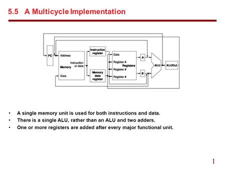
Model 2: Augmenting the Single Cycle MIPS Datapath to Consolidate the ALUs
Questions
- Why does the multicycle approach use only a single ALU? Why was this impossible with the single cycle design?
- How does an add instruction execute through this datapath? Hint: it requires multiple steps through the datapath now!
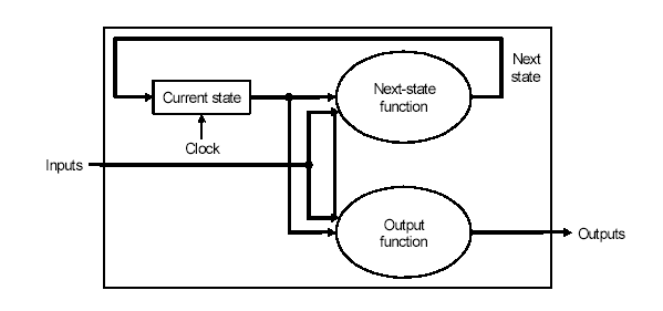
Model 3: Modifying the Control Unit to Output Specialized Control Signals at Each Instruction Stage via a Finite State Machine
| Fetch | Decode | ALU | Memory Access | Writeback |
|---|---|---|---|---|
| IR = Mem[PC] | A = Reg[rs] | lw/sw: ALUOut = A+immediate (IR[15:0]) | lw: MDR = Mem[ALUOut] | lw/sw: Reg[rt] = MDR |
| ALUOut = PC + 4 | B = Reg[rt] | R type: ALUOut = func | sw: Mem[ALUOut] = B | R-type: Reg[rd] = ALUOut |
| PC += 4 | ALUOut = immediate (IR[15:0]) <<2 sign extended to 32 bits |
beq: ALUOut = A - B; if zero, PC = ALUOut | R-type: skip to writeback | |
| j: PC = jump target |
Questions
- Describe the functionality of each control signal in this datapath, for each instruction cycle stage.
- How does the conditional and boolean logic of the multi-cycle control unit differ from that of the single cycle control? In other words, what additional input(s) are needed to the control unit to determine the output control bits, beyond merely the opcode and function code?
Model 4: The MIPS Multicycle Datapath
Questions
- Trace an add, beq, and j instruction through this datapath.
- Add an instruction to the datapath and control finite state machine flowchart to support
blez: branch if less than or equal to 0.
Model 5: Calculating Performance via Cycles Per Instruction (CPI)
| Opcode | Instruction Fetch | Regiter Read | ALU | Memory | Register Writeback | Total Time (ps) |
|---|---|---|---|---|---|---|
| R | 200 | 50 | 100 | 0 | 50 | 400 |
| lw | 200 | 50 | 100 | 200 | 50 | 600 |
| sw | 200 | 50 | 100 | 200 | 0 | 550 |
| beq | 200 | 50 | 100 | 0 | 0 | 350 |
| j | 200 | 0 | 0 | 0 | 0 | 200 |
Questions
- How many cycles are required for each instruction above? Hint: use the control unit finite state machine and count the length of each path.
- Suppose a program has 25% loads, 10% stores, 52% ALU instructions, 11% branches, and 2% jumps. What is the average number of cycles per instruction?
- The average cycles per instruction for the single cycle datapath is always 1. Why is this an improvement? Hint: consider the timing length of each cycle for single cycle and for multi cycle.
Model 6: Key Formulas and Concepts Recap
A one-page summary of the multicycle design.
Key formulas and rules:
| Formula / Rule | Micro-example |
|---|---|
| Each instruction is broken into steps (fetch, decode, ALU, memory, writeback), one short clock cycle per step. | The clock only needs to fit the slowest step (e.g. 200 ps), not the slowest instruction |
| Different instructions take different numbers of cycles. | lw = 5, sw = 4, R type = 4, beq = 3, j = 3 |
| Average CPI = sum over instruction types of (frequency × cycles). | 25% × 5 + 10% × 4 + 52% × 4 + 11% × 3 + 2% × 3 = 1.25 + 0.40 + 2.08 + 0.33 + 0.06 = 4.12 |
| Execution time = instruction count × CPI × clock period. | 100 × 4.12 × 200 ps = 82,400 ps (vs. 100 × 1 × 600 ps = 60,000 ps single cycle -- compare carefully!) |
| Hardware is reused across cycles: one ALU serves PC + 4, address arithmetic, comparisons, and branch targets. | Cycle 1: ALU computes PC + 4; cycle 3: the same ALU adds base + offset for lw |
| Intermediate results must be latched in new registers between cycles. | IR (instruction), A and B (register reads), ALUOut, MDR (memory data) |
| Control becomes a finite state machine: the control outputs depend on the opcode and the current step. | State 0 (fetch) always reads memory; a later state asserts RegWrite only for lw/R types |
Cycles per instruction at a glance:
| Instruction | Fetch | Decode | ALU | Memory | Writeback | Total cycles |
|---|---|---|---|---|---|---|
| lw | 1 | 1 | 1 | 1 | 1 | 5 |
| sw | 1 | 1 | 1 | 1 | - | 4 |
| R type | 1 | 1 | 1 | - | 1 | 4 |
| beq | 1 | 1 | 1 | - | - | 3 |
| j | 1 | 1 | 1 | - | - | 3 |
Glossary:
| Term | One-line definition |
|---|---|
| Multicycle design | A datapath where each instruction takes several short clock cycles, one per step. |
| CPI | Cycles per instruction; a weighted average over the instruction mix in multicycle designs. |
| Finite state machine (FSM) | A controller that moves through states cycle by cycle, emitting different control signals in each. |
| Instruction register (IR) | Latches the fetched instruction so its fields remain available in later cycles. |
| MDR | Memory data register: latches data read from memory for use in the writeback cycle. |
| ALUOut | A register holding the ALU's result between cycles (e.g. a load's effective address). |
| A and B registers | Latches holding the values read from rs and rt during the decode cycle. |
| State | One step of the control FSM; the current state plus the opcode determines the next state. |